Fused-Silica Wafer Machining
Process-development structures written into and onto transparent fused silica while commissioning the motion, focus, exposure, and imaging behaviour of the fabrication platform.
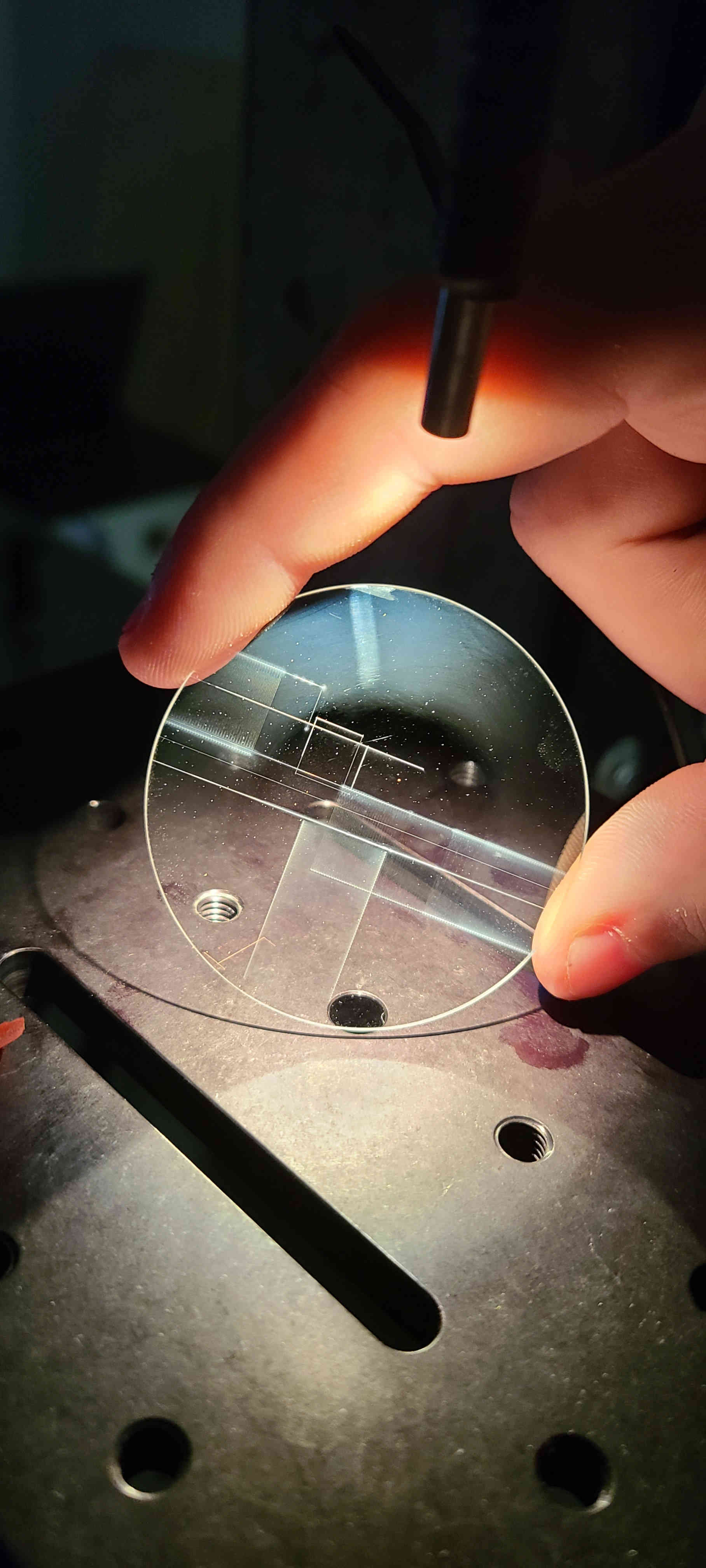
Using the sample as a record of the process.
Fused silica is transparent at common near-infrared inscription wavelengths, allowing focused femtosecond pulses to modify material at the surface or within the bulk through nonlinear absorption. The resulting response changes sharply with focus, pulse energy, repetition rate, scan velocity, polarization, and exposure history.
Patterned wafers provide a convenient way to map those variables while checking the machine itself. Straight lines reveal motion and focus stability; repeated structures expose timing or backlash; two-dimensional fields show overlap, heat accumulation, and debris behaviour.
Separate machine behaviour from material response.
Early process tests are designed to identify whether a defect originates in the optical focus, stage trajectory, pulse delivery, sample mounting, or the interaction physics itself. Repeating simple geometries while changing one variable at a time creates a practical baseline for more complex fabrication.
- Locate the surface and establish a repeatable focal reference.
- Map modification and ablation thresholds over pulse energy and scan speed.
- Check line straightness, spacing, corner behaviour, and bidirectional scan consistency.
- Compare single-pass and repeated-pass exposure to identify cumulative damage.
- Inspect structures optically to relate visible morphology to the programmed path.
A compact diagnostic for the entire inscription chain.
Surface and bulk structures make errors visible. A changing line width may indicate focal drift or energy instability; nonuniform spacing may identify motion or trigger timing; asymmetric edges can reveal scan-direction effects; and unexpected cracking or debris marks an excessive energy-density regime.
These results inform safe and repeatable operating windows before moving to optical-fibre inscription, where the target region is smaller and the performance consequences may only become apparent after spectral measurement.
From test patterns to functional structures.
The same platform can extend from surface ablation to embedded refractive-index structures, optical waveguides, periodic nonlinear modifications, microfluidic precursors, and three-dimensional features. Process maps from the wafer trials provide the starting point for those more sensitive fabrication regimes.